Daily Image
02-08-2007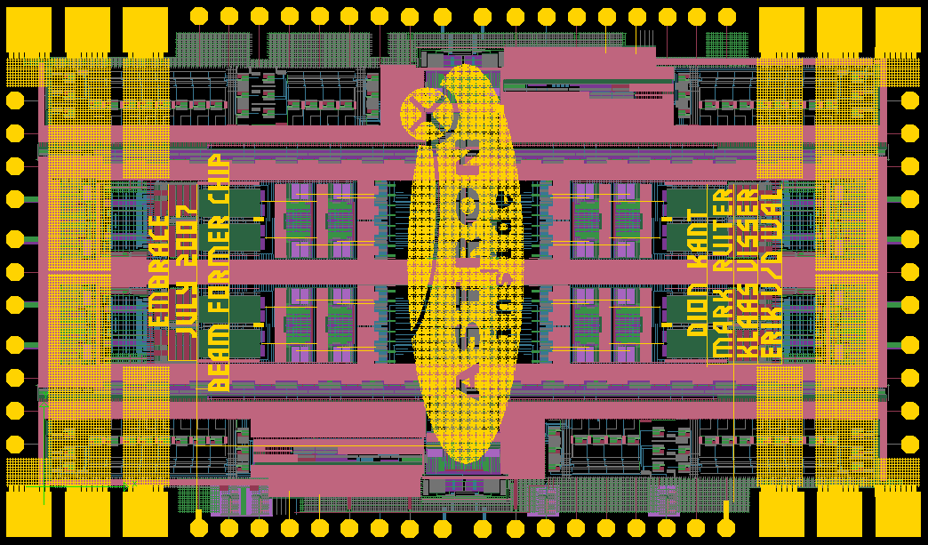
The EMBRACE design team beats management bet!
| Submitter: | Klaas Visser |
| Description: | Despite ongoing bets within ASTRON, the EMBRACE design team succeeded in performing a tape-out of the beam-former chip before the dead-line on July 31. The team needed to work late lots of evenings as well as weekends, but fortunately we managed it. The beam-former chip is an analogue RF integrated circuit (RFIC), which is an essential part for aperture array technology. The main function of the chip is to combine the four input signals, coming from the antennas, into two independent beams. The signal chain of this chip includes a low noise dual feedback amplifier, poly-phase networks, switching networks, amplitude correction facility as well as output drivers. All settings of the chip are under full digital control, through an SPI interface. A total of 40 buffered registers, are then interfaced internally to the analogue part. Some registers are combined as input for D/A-conversion. The whole system on chip design is based on a differential paradigm. This beam-former chip will replace roughly 90 percent of the electronics on the current EMBRACE prototype boards. Apart from gain stages it replaces 8 KDI vector modulators, as were used in the THEA demonstrator. The analogue processing power of the chip can be expressed in the equivalent number of Flops, as a digital solution would need to perform a similar task. A conservative number leads to 24 GFlops of processing power. The chip was designed in the SG25H1 process of IHP-microelectronics. This process is a 0.25 µm SiGe:C BiCMOS technology, with npn Hetero-junction bipolar transistors with an fT and fmax of respectively 180 and 220 GHz. Some key figures to indicate the complexity of the design: 12480 SiGe Hetero-junction bipolar transistors 17745 CMOS transistors 136314 connections 12.6 square millimeters die size The design was made using a combination of Cadence and Agilent ADS software on two dual Xeon workstations equipped with 8GByte RAM each. At the end the design database consumed roughly 400 GBytes of disk space and both systems were fully stressed to their limits. Verification jobs running in parallel for more than 8 hours and using 4 GByte RAM each were not exceptional. Dion Kant, Mark Ruiter, Erik van der Wal, Klaas Visser |
| Copyright: | (C) Parbhu Patel 2007 |
| Tweet |  |