Daily Image
31-08-2007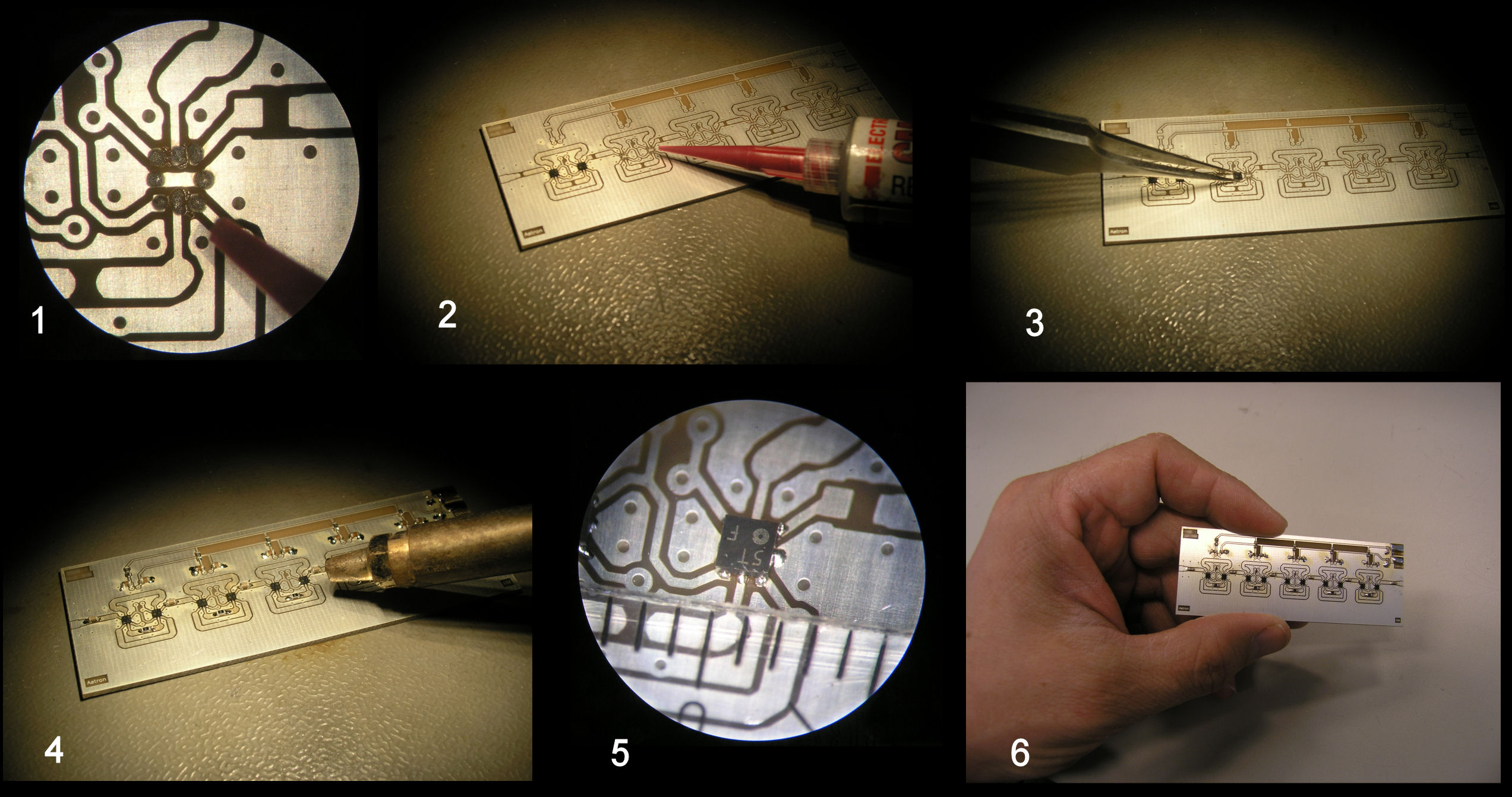
Miniaturization of electronic components
| Submitter: | Henri Meulman |
| Description: | The smaller, the better, they always say. Then one can cram more components on a square centimeter PCB (Printed Circuit Board), so an electronic device can be smaller, or more complex, or cheaper. But smaller is not better when one has to solder the components on the board by hand. A normal soldering iron is not useful anymore. Fortunately a technique has been developed to overcome this problem, although this technique also has its limits. This picture shows an electronic component with a size of 1.5 X 1.5 millimeters, with 8 solder connections. Soldering this kind of component takes some skill because the pads on the PCB on which it is to be soldered are more than 5 times smaller than a regular 0603 component. Picture 1 and 2: With a dispenser, solder paste is placed on the pads on which the component is to be soldered. This is the tricky part. Too much paste will result in a short circuit between two pads. To little paste, and no connection will be made between the pin of the component and the pad. Picture 3: Placing the component (with the correct orientation, of course). Picture 4: The actual soldering. With hot air (over 300 degrees), the paste is turned into liquid tin. In this way, it is also possible to solder underneath the component. Picture 5: When the component has cooled down, the quality of the solder connection can be tested. (NB: The ruler shows mm, not cm)! Picture 6: The PCB is ready to use . |
| Copyright: | Astron |
| Tweet |  |