Daily Image
14-11-2007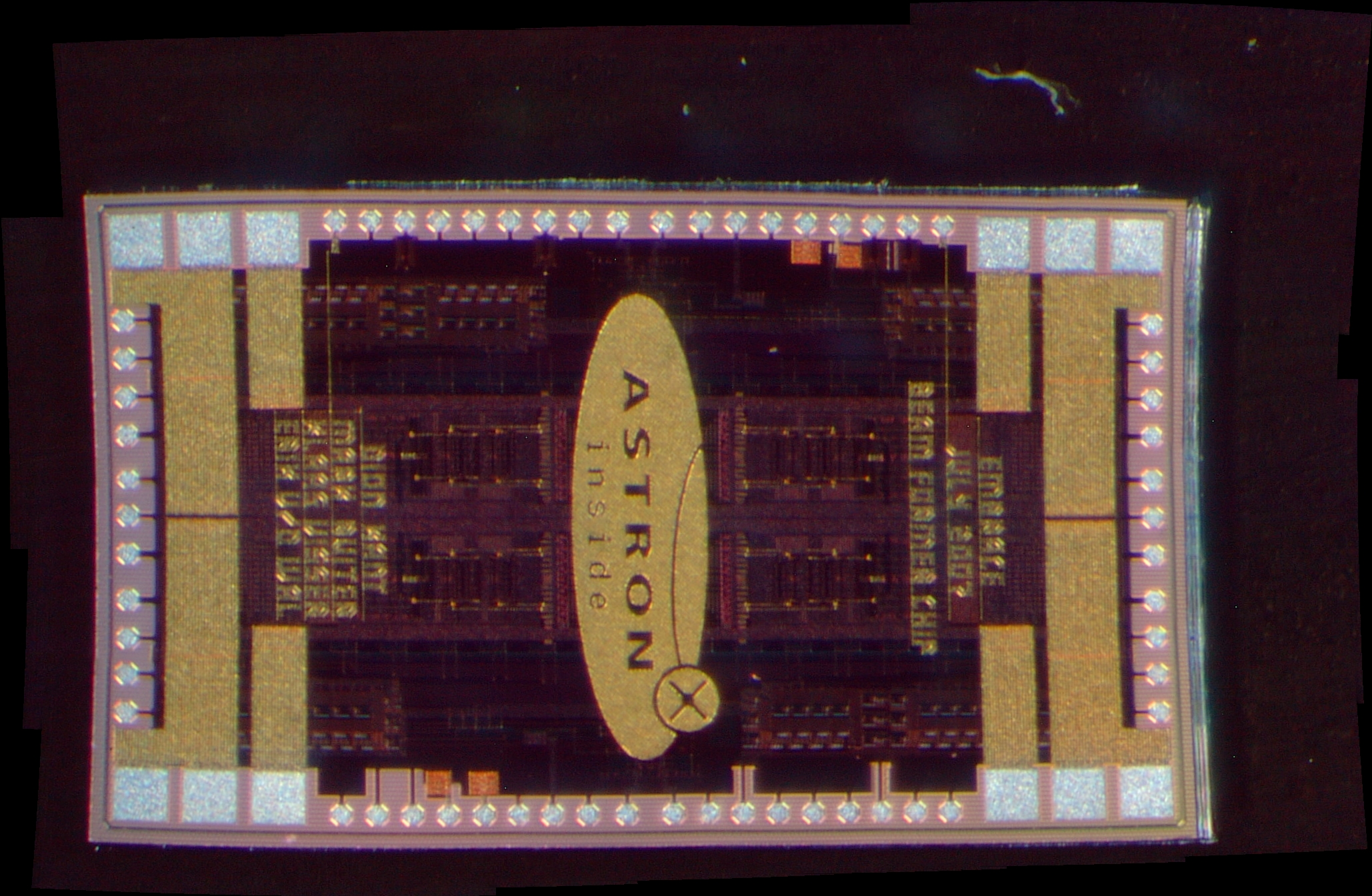
MICROSCOPE IMAGE OF THE FULL EMBRACE BEAM-FORMER CHIP
| Submitter: | EMBRACE project team |
| Description: | The picture shows a photograph of the EMBRACE beam-former chip, captured through a microscope. Actually this is a combination of several pictures since the field of view (FoV) of the microscope is very limited. Fortunately, the FoV provided by the beam former chip in the EMBRACE system will be gigantic when it is compared to other radio astronomy concepts. The chip provides a means for combining the signals from four array antenna elements into two independent beams. It includes an efficient digital serial interface for controlling the beams. This high scale integrated circuit combines analogue RF and digital electronics and it will replace roughly 90 percent of the electronics of conventional (non integrated) phased array front-end circuitry. The chip was designed in the SG25H1 process of IHP-microelectronics. This process is a 0.25 µm SiGe BiCMOS technology with npn Hetero-junction bipolar transistors with an fT and fmax of 180 and 220 GHz respectively. The actual chip size is 4.6 mm by 2.7 mm. In this area 12480 SiGe Hetero-junction bipolar transistors and 17745 CMOS transistors are integrated. On the periphery of the chip the bonding pads are clearly visible. The larger pads are for the power supply. The other prominently visible layer is the top level metal layer in which a.o. the ASTRON logo is created. Next, some samples are bonded in-house before the actual measurements can begin. Also 20 units are shipped for male bonding in small QFP-packages by an external company. Several test dies are available. We have the primary dies with the full beam-former chip, but we also have several sub-blocks which can be tested separately. One such sub-block contains a so-called one-channel beam-former. At ASTRON we begin by bonding a one-channel unit as a naked die, directly on a test PCB. We await the results of the measurements of the one-channel beam-former unit. Only then can we decide if the chip performs as it is designed. This work is performed within the SKADS framework and it is supported by ASTRON and the EU 6th framework programme. |
| Copyright: | Copyright (C), ASTRON 2007 |
| Tweet |  |