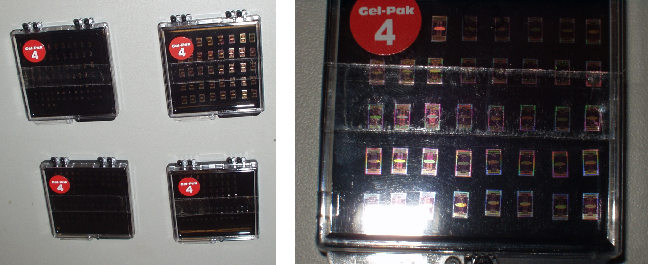
| Description: | At the end of July, the EMBRACE team had 'tape-out' of the ASTRON beamformer chip for EMBRACE. This means that a file with all the design data in it (in GDS2 format) was sent to an IC foundry for processing the silicon. Our design was part of a so-called multi-project wafer, which is a common way for sharing the large costs of an IC processing run among the participating projects on the wafer. After processing, the wafers are diced up, and the resulting naked dies from the wafers are packaged into boxes before sending the silicon back to the participants.
The boxes with the silicon dies are shown in the picture. They were received in good order on October 26th. Next, the chips will be tested. Measurements will be compared to the behaviour that is predicted by the simulation models. In a next report we will update on more details. This work is performed within the SKADS framework and it is supported by ASTRON and the EU 6th framework programme.
|